Patents - EUON
ICT
Overview
This section looks at the patenting activity in the field of nanotechnology and agriculture in 2017-2020. Granted patents and patent applications focused on agriculture and nanotechnology were extracted from the general collection of nanotechnology patents in 2017-2020 developed by the study team for the database. The patents were collected from Espacenet database maintained by the European Patent Office.
The dataset of patents on agriculture and nanotechnology was developed by extracting the granted patents and patent applications that contained the CPC classes and sub-classes dedicated to information and communication technology in their bibliographic information. It should be noted that most nanotechnology patents contain multiple classes in their subject descriptions. In CPC information and communication technology is covered under G16 class (Information and Communication Technology (ICT) specially adapted for specific application field), while nanotechnology applications for information processing – under sub-classes of B82Y (Nanotechnology).
| Table AVII-3: ICT in the Cooperative Patent Classification (CPC)1 | |
|---|---|
| Class | Title |
| G16B | Bioinformatics, i.e. information and communication technology [ICT] specially adapted for genetic or protein-related data processing in computational molecular biology |
| G16C | Computational chemistry; chemoinformatics; computational materials science |
| G16H | Healthcare informatics, i.e. information and communication technology [ICT] specially adapted for the handling or processing of medical or healthcare data |
| G16Y | Information and communication technology specially adapted for the Internet of Things [IoT] |
| G16Z | Information and communication technology [ICT] specially adapted for specific application fields, not otherwise provided for |
| B82Y10/00 | Nanotechnology for information processing, storage or transmission, e.g. quantum computing or single electron logic |
ICT in nanotechnology patents
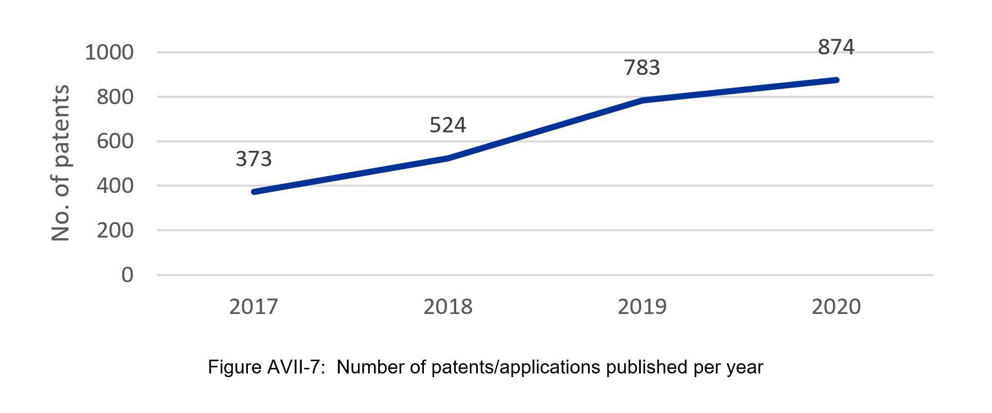
As a result of patent collection mining, 2554 patent applications and granted patents published in 2017-2020 were identified. The number of patents and patent applications containing ICT steadily increased over the whole period.

Most patents (1949, 76%) were published in the national patent offices, while the rest – in World Intellectual Property Organisation (WIPO, 527, 21%) and the European Patent Office (78, 3%).
USA (1138 applications, 45%) prevailed among the countries where most patent applications were published. It was followed by China (448, 18%). Other countries, such as South Korea, Taiwan and Japan that were in top five by the number of published applications significantly lagged behind the USA.
| Table AVII-4: Top five countries by filed patents/applications in agriculture and nanotechnology in 2017-2020 | |
|---|---|
| Country | No. of patents/patent applications, % |
| USA | 1138, 45 |
| China | 448, 18% |
| South Korea | 163, 6% |
| Taiwan | 80, 3% |
| Japan | 32, 1% |
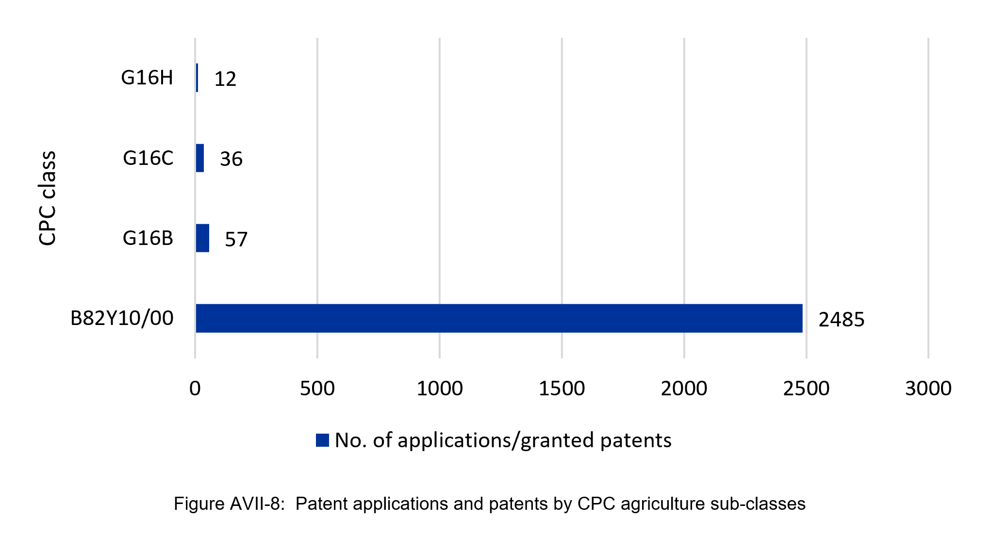
Patent applications and granted patents contained four CPC sub-classes referring to ICT and nanotechnology. One patent application might combine several ICT-related CPC sub-classes.

The overwhelming majority of patents and applications focused on applications of nanotechnology in for information processing, storage or transmission, e.g., quantum computing or single electron logic (B82Y10/00) – 2485 (97%) patents/applications. Other fields received substantially less attention; so they visibility could not be considered significant.
Other classes (e.g., nanotechnology and internet of things or other applications) were not identified in the collection of patents and applications published in 2017-2020.
| Table AVII-5: Examples of patents focused on B82Y10/00 sub-class | |
|---|---|
| Bibliographic information | Abstract |
| Li, T. Y., Yu, S.-M. (2019). Spacers for nanowire-based integrated circuit device and method of fabricating same. Patent no. US10475902B2. Available here. (Granted patent) |
Nanowire-based integrated circuit devices and methods for fabricating such are disclosed herein. An exemplary method includes forming a heterostructure over a substrate. A gate structure is formed traversing the heterostructure, such that the gate structure separates a source region and a drain region of the heterostructure and defines a channel region between the source region and the drain region. A source/drain nanowire release process is performed on the heterostructure to release a nanowire in the source region and the drain region. Nanowire spacers are then formed in the source region and the drain region. The nanowire is disposed between the nanowire spacers. During a gate replacement process, a channel nanowire release process is performed on the heterostructure to release the nanowire in the channel region. Epitaxial source/drain features are formed over the nanowire and the nanowire spacers in the source region and the drain region before the gate replacement process. |
| Brink, M. et al. (2020). Qubit network non-volatile identification. Patent no. US10608157B2. Available here. (Granted patent) |
A technique relates to a superconducting chip. Resonant units have resonant frequencies, and the resonant units are configured as superconducting resonators. Josephson junctions are in the resonant units, and one or more of the Josephson junctions have a shorted tunnel barrier. |
ICT innovation breakthroughs in patents
Innovation breakthrough is a peculiar type of innovation that has a profound effect on on subsequent inventions, products and services. Three indicators of patents were studied to identify innovation breakthroughs – number of forward citations, number of citing organisations and number of citing countries. Thirty-two patents/applications of 48 identified breakthrough referred to the ICT field.
| Table AVII-6: ICT breakthrough patents and patent applications published 2017-2020 | |||
|---|---|---|---|
| Bibliographic data | No. of citations | No. of citing organisations | No. of citing countries |
| Balakrishnan, K. et al. (2017). Replacement III-V or germanium nanowires by unilateral confined epitaxial growth. No. US9570551B1. IBM. Available here. | 33 | 7 | 4 |
| Bi, Z. et al. (2019). Buffer regions for blocking unwanted diffusion in nanosheet transistors. IBM. No. US10263100B1. Available here. | 24 | 9 | 6 |
| Cheng, K. et al. (2018). Inner spacer for nanosheet transistors. IBM. No. US9923055B1. Available here. | 21 | 6 | 5 |
| Kim D.-W. et al. (2017). Semiconductor device. Samsung Electronics. No. US2017250261A1. Available here. | 18 | 6 | 4 |
| Leobandung, E. et al. (2017). Self-aligned replacement metal gate spacerless vertical field effect transistor. IBM. No. US2017222045A1. Available here. | 16 | 6 | 5 |
| Elsherbini, A. et al. (2019). Quantum computing assemblies. Intel Corporation. No. US10380496B2. Available here. | 16 | 3 | 2 |
| Veneziano, R. et al. (2017). Stable nanoscale nucleic acid assemblies and methods thereof. No. WO2017189870A1. Massachusetts Institute of Technology. Available here. | 15 | 13 | 5 |
| Cheng, K. et al. (2017). iFinFET. IBM. No. US9728621B1. Available here. | 14 | 7 | 6 |
| Chang, J. et al. (2017). Local germanium condensation for suspended nanowire and FINFET devices. IBM. No. US2017005190A1. Available here. | 14 | 6 | 3 |
| Balakrishnan, K. et al. (2017). Strained stacked nanowire field-effect transistors (FETs). IBM. No. US2017077232A1. Available here. | 13 | 6 | 5 |
| Mochizuki, S. et al. (2018). Gate metal patterning for tight pitch applications. IBM. No. US10103065B1. Available here. | 13 | 4 | 4 |
| Roberts, J. et al. (2018). Controlled current flux bias lines in qubit devices. Intel Corporation. No. WO2018182571A1. Available here. | 13 | 3 | 2 |
| Bathe, M. et al. (2017). Sequence-controlled polymer random access memory storage. Massachusetts Institute of Technology. No. WO2017189914A1. Available here. | 11 | 7 | 3 |
| Cheng, K. et al. (2018). Integrating thin and thick gate dielectric nanosheet transistors on same chip. IBM. No. US10141403B1. Available here. | 11 | 5 | 4 |
| Caudillo, R. et al. (2019). Qubit devices with undercut conductive circuit elements. Intel Corporation. No. WO2019032114A1. Available here. | 11 | 3 | 2 |
| Thomas, N. et al. (2018). On-chip control logic for qubits. Intel corporation. No. WO2018063206A1. Available here. | 10 | 5 | 3 |
| Chung, W. K. et al. (2018). Semiconductor device and method for fabricating the same. Samsung Electronics. No. US2018130905A1. Available here. | 10 | 5 | 4 |
| Lampert, L. et al. (2019). Wafer-scale integration of dopant atoms for donor- or acceptor-based spin qubits. Intel Corporation. No. US2019043968A1. Available here. | 10 | 4 | 2 |
| Ando, T. et al. (2019). Stacked field-effect transistors (FETs) with shared and non-shared gates. IBM. No. US10236217B1. Available here. | 10 | 5 | 5 |
| Cheng, K. et al. (2019). Integrating standard-gate and extended-gate nanosheet transistors on the same substrate. IBM. No. US10243054B1. Available here. | 10 | 5 | 5 |
| Brink, M. et al. (2019). Bumped resonator structure. IBM. No. US10263170B1. Available here. | 9 | 4 | 2 |
| Ando, T. et al. (2019). Gate formation scheme for nanosheet transistors having different work function metals and different nanosheet width dimensions. IBM. No. US10490559B1. Available here. | 9 | 4 | 4 |
| Leobandung, E. et al. (2018). Fabrication of nanowire vertical gate devices. IBM. No. US10062752B1. Available here. | 8 | 6 | 6 |
| Cheng, K. et al. (2019). Integration of thick and thin nanosheet transistors on a single chip. IBM. No. US10229971B1. Available here. | 8 | 5 | 5 |
| Cheng., K. et al. (2019). Nanosheet transistor. IBM. No. US10243061B1. Available here. | 8 | 4 | 2 |
| Roberts, J. et al. (2018). Superconducting qubit device packages. Intel Corporation. No. WO2018125026A1. Available here. | 7 | 4 | 4 |
| Thomas, N. et al. (2019). Quantum dot devices with overlapping gates. Intel Corporation. No. US2019043952A1. Available here. | 7 | 3 | 2 |
| Elsherbini, A. et al. (2019). Quantum computing assemblies. Intel Corporation. No. WO2019132963A1. Available here. | 6 | 4 | 2 |
| Seo, S.-C. et al. (2019). Source and Drain Isolation for CMOS Nanosheet with One Block Mask. IBM. No. US10325820B1. Available here. | 5 | 4 | 4 |
| Miao, X. et al. (2019). Nanosheet transistor with high-mobility channel. IBM. No. US10424639B1. Available here. | 5 | 3 | 3 |
| Gaznhorn, M. et al. (2019). Cross-talk compensation in quantum processing devices. IBM. No. US10452991B1. Available here. | 5 | 3 | 2 |
| Ando, T. et al. (2019). Method and structure to introduce strain in stack nanosheet field effect transistor. IBM. No. US10332809B1. Available here. | 4 | 3 | 3 |
1 European Patent Office. (2022). Cooperative Patent Classification, A: Human necessities agriculture. Available at: https://www.cooperativepatentclassification.org/sites/default/files/cpc/scheme/A/scheme-A.pdf


