Patents - EUON
Photonics
Overview
This section looks at the patenting activity in the field of nanotechnology and photonics in 2017-2020. Granted patents and patent applications focused on photonics and nanotechnology were extracted from the general collection of nanotechnology patents in 2017-2020 developed by the study team for the database. The patents were collected from Espacenet database maintained by the European Patent Office.
The dataset of patents on photonics and nanotechnology was developed by extracting the granted patents and patent applications that contained the CPC classes and sub-classes dedicated to photonics in their bibliographic information. It should be noted that most nanotechnology patents contain multiple classes in their subject descriptions. In CPC photonics is covered under B82Y20/00 class ‘Nano-optics, e.g. quantum optics or photonic crystals’1. Nano-photonics and nanooptics are synonyms that refer to the discipline focused on the investigation of ‘the behaviour of light on nanometre scales as well as interactions of nanometre-sized objects with light’.2
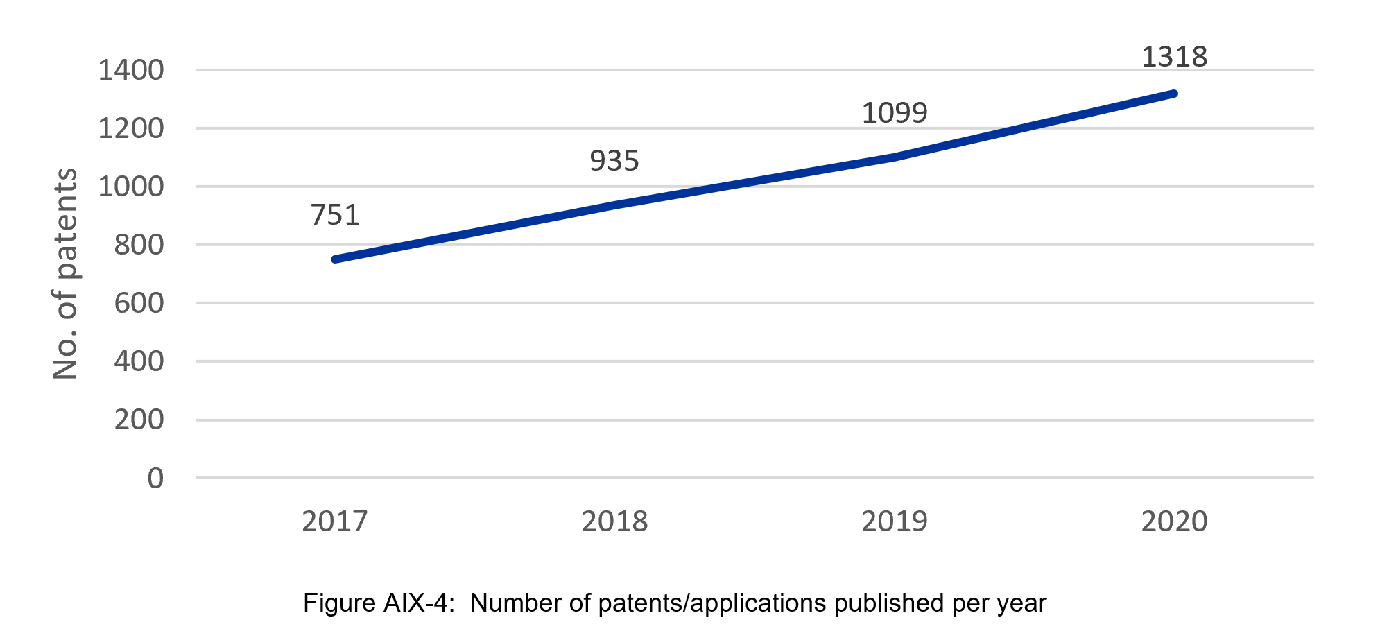
Patents on nanotechnology in Photonics
As a result of patent collection mining, 4103 patent applications and granted patents published in 2017-2020 were identified. The number of patents and patent applications containing photonics classifications steadily increased each year.
Most patents (3241, 79%) were published in the national patent offices, while the rest – in World Intellectual Property Organisation (WIPO, 763, 19%) and the European Patent Office (99, 2%).
China (2261 applications, 55%) prevailed among the countries where most patent applications were published. Other countries, such as USA, South Korea, Japan and Taiwan that were in top five by the number of published applications significantly lagged behind China.
| Table AV-3: Top five countries by filed patents/applications in environment and nanotechnology in 2017-2020 | |
|---|---|
| Country | No. of patents/patent applications, % |
| China | 2261, 55% |
| USA | 547, 14% |
| South Korea | 237, 6% |
| Japan | 61, 2% |
| Taiwan | 48, 1% |
Patent applications and granted patents contained only one CPC sub-class referring to photonics. One patent application might combine several CPC sub-classes related to health, ICT and other fields.
| Table AIX-3: Examples of patents focused on B82Y20/00 sub-class | |
|---|---|
| Bibliographic information | Abstract |
| Abel, S.; Seidler, P. (2017). One-dimensional photonic crystal with pillars having a layer structure. Patent no. US9715158B1. Available here. | The present invention is notably directed to a (quasi) one-dimensional photonic crystal cavity. This cavity comprises a set of aligned pillars, where the pillars are embedded in a cladding. At least one of the pillars has a sandwich structure, wherein a layer of nonlinear optical material is between two layers of materials having, each, a refractive index that is higher than the refractive index of the nonlinear optical material. The invention can furthermore be embodied as an all-optical modulator or an all-optical transistor, comprising a photonic crystal such as described above. Finally, the invention is further directed to methods for modulating an optical signal, using such a photonic crystal cavity. |
| Kong, X. et al. (2017). Satellite-borne ray-energy nanobattery. Patent no. CN106409955A. Available here. | Provided in the invention is a satellite-borne ray-energy nanobattery comprising silicon nanowires, a caesium iodide layer, a bulk silicon emitter, an exhaustion region, a bulk silicon base and a back panel. The silicon nanowires absorb light from an ultraviolet band, a visible band and an infrared band to generate free electrons; and the photon energy is collected by the silicon nanowires, thereby increasing the power density. The caesium iodide layer absorbs a high-energy X ray and a high-energy gamma ray and converts the high-energy ray photon into a photo at the visible band. The bulk silicon emitter and the bulk silicon base collect excessive carriers and absorb perpendicular incidence and secondary reflection photons. A built-in voltage is kept in the exhaustion region to guarantee separation of a photon-generated carrier. The back panel reflects the photons and the photo absorbing probability by the bulk silicon is increased. According to the invention, the surface coating structure of the solar cell is made of a caesium-iodide scintillation crystal material and the response band of eh current solar battery is broadened to the ray region including the x ray and the gamma ray, so that a certain radiation damage protection effect is realized. And thus, the power supply demand of the spacecraft in a high-radiation low-illumination space environment can be satisfied. |
Photonics innovation breakthroughs in patents
Innovation breakthrough is a peculiar type of innovation that has a profound effect on on subsequent inventions, products and services. Three indicators of patents were studied to identify innovation breakthroughs – number of forward citations, number of citing organisations and number of citing countries.
Seven patents/applications met the requirements of innovation breakthroughs in photonics. Five patents/applications were published by Samsung Electronics Co. Ltd. (South Korea), while two – by Boe Technology Group Co. Ltd. (China) and University of California (USA).
| Table AIX-4: Photonics breakthrough patents and patent applications published in 2017-2020 | ||||
|---|---|---|---|---|
| Bibliographic data | No. of citations | No. of citing organisations | No. of citing countries | |
| He, X. et al. (2017). Display device and fabricating method. Boe Technology Group Co. Ltd. No. US2017229429A1. Available here. | 12 | 8 | 5 | |
| Zhang, J. et al. (2017). Co-doped core/shell nanocrystals for visible light emission. University of California. No. WO2017019789A1. Available here. | 11 | 6 | 4 | |
| Han, S. et al. (2017). Optical modulator including nanostructure. Samsung Electronics Co. Ltd. No. US2017023803A1. Available here. | 11 | 6 | 5 | |
| You, J. et al. (2019). Projector including meta-lens. Samsung Electronics Co. Ltd. No. US2019139243A1. Available here. | 10 | 3 | 3 | |
| Chung, D. et al. (2018). Layered structures, production methods thereof, and liquid crystal display including the same. Samsung Electronics Co. Ltd. No. Available here. | 9 | 5 | 4 | |
| Park, S. H. et al. (2018). Quantum dots, a composition or composite including the same, and an electronic device including the same. Samsung Electronics Co. Ltd. No. CN108102640A. Available here. | 8 | 4 | 2 | |
| Yoo, J. et al. (2019). Reflective display device. No. US2019196267A1. Available here. | 4 | 3 | 3 | |
1 European Patent Office. (2022). Cooperative patent classification, B: Specific uses or applications of nanostructures; measurement or analysis of nanostructures; manufacture or treatment of nanostructures. Available at: https://www.cooperativepatentclassification.org/sites/default/files/cpc/scheme/B/scheme-B82Y.pdf
2 Nasrollahzadeh, M. (2019). Chapter 2 - Types of nanostructures. In An Introduction to Green Nanotechnology. Elsevier.